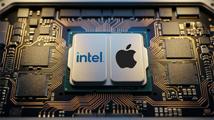
The semiconductor industry has officially entered the "Angstrom Era," a transition marked by a radical architectural shift that flips the traditional logic of chip design upside down—quite literally. As of January 16, 2026, the long-anticipated deployment of Backside Power Delivery (BSPD) has moved from the research lab to high-volume manufacturing. Spearheaded by Intel (NASDAQ: INTC) and its PowerVia technology, followed closely by Taiwan Semiconductor Manufacturing Co. (NYSE: TSM) and its Super Power Rail (SPR) implementation, this breakthrough addresses the "interconnect bottleneck" that has threatened to stall AI performance gains for years. By moving the complex web of power distribution to the underside of the silicon wafer, manufacturers have finally "de-cluttered" the front side of the chip, paving the way for the massive transistor densities required by the next generation of generative AI models.
The significance of this development cannot be overstated. For decades, chips were built like a house where the plumbing and electrical wiring were all crammed into the ceiling, leaving little room for the occupants (the signal-carrying wires). As transistors shrunk toward the 2nm and 1.6nm scales, this congestion led to "voltage droop" and thermal inefficiencies that limited clock speeds. With the successful ramp of Intel’s 18A node and TSMC’s A16 risk production this month, the industry has effectively moved the "plumbing" to the basement. This structural reorganization is not just a marginal improvement; it is the fundamental enabler for the thousand-teraflop chips that will power the AI revolution of the late 2020s.
The Technical "De-cluttering": PowerVia vs. Super Power Rail
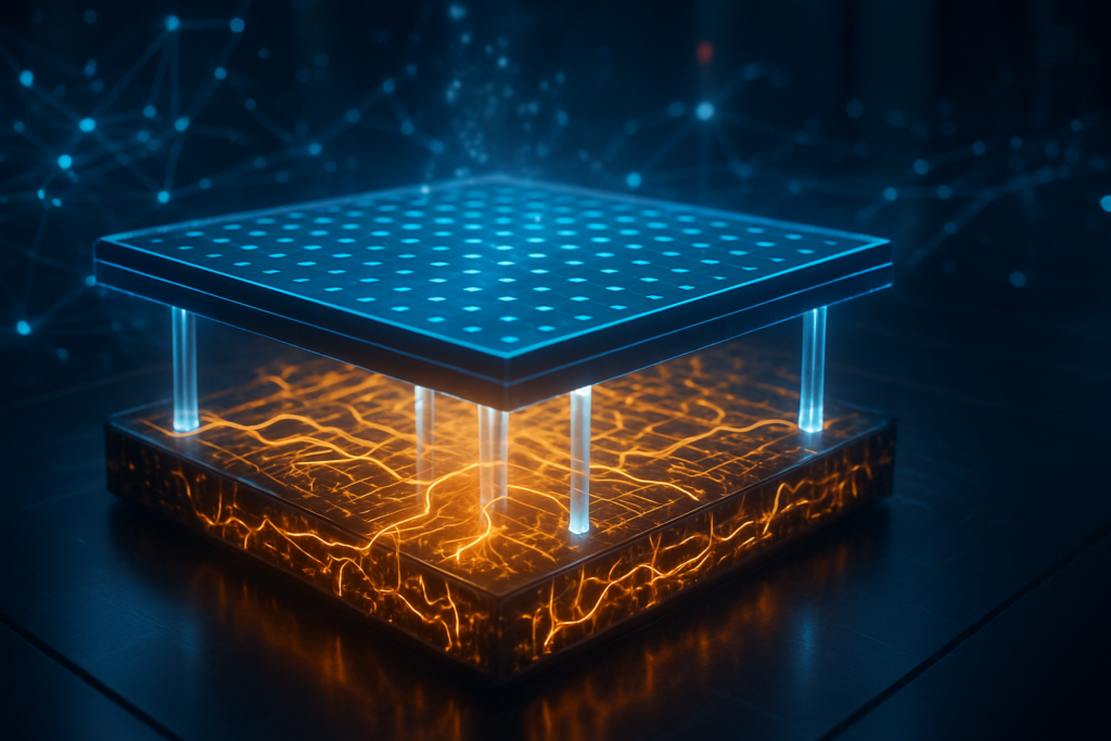
At the heart of this shift is the physical separation of the Power Distribution Network (PDN) from the signal routing layers. Traditionally, both power and data traveled through the Back End of Line (BEOL), a stack of 15 to 20 metal layers atop the transistors. This led to extreme congestion, where bulky power wires consumed up to 30% of the available routing space on the most critical lower metal layers. Intel's PowerVia, the first to hit the market in the 18A node, solves this by using Nano-Through Silicon Vias (nTSVs) to route power from the backside of the wafer directly to the transistor layer. This has reduced "IR drop"—the loss of voltage due to resistance—from nearly 10% to less than 1%, ensuring that the billion-dollar AI clusters of 2026 can run at peak performance without the massive energy waste inherent in older architectures.
TSMC’s approach, dubbed Super Power Rail (SPR) and featured on its A16 node, takes this a step further. While Intel uses nTSVs to reach the transistor area, TSMC’s SPR uses a more complex direct-contact scheme where the power network connects directly to the transistor’s source and drain. While more difficult to manufacture, early data from TSMC's 1.6nm risk production in January 2026 suggests this method provides a superior 10% speed boost and a 20% power reduction compared to its standard 2nm N2P process. This "de-cluttering" allows for a higher logic density—TSMC is currently targeting over 340 million transistors per square millimeter (MTr/mm²), cementing its lead in the extreme packaging required for high-performance computing (HPC).
The industry’s reaction has been one of collective relief. For the past two years, AI researchers have expressed concern that the power-hungry nature of Large Language Models (LLMs) would hit a thermal ceiling. The arrival of BSPD has largely silenced these fears. By evacuating the signal highway of power-related clutter, chip designers can now use wider signal traces with less resistance, or more tightly packed traces with less crosstalk. The result is a chip that is not only faster but significantly cooler, allowing for higher core counts in the same physical footprint.
The AI Foundry Wars: Who Wins the Angstrom Race?
The commercial implications of BSPD are reshaping the competitive landscape between major AI labs and hardware giants. NVIDIA (NASDAQ: NVDA) remains the primary beneficiary of TSMC’s SPR technology. While NVIDIA’s current "Rubin" platform relies on mature 3nm processes for volume, reports indicate that its upcoming "Feynman" GPU—the anticipated successor slated for late 2026—is being designed from the ground up to leverage TSMC’s A16 node. This will allow NVIDIA to maintain its dominance in the AI training market by offering unprecedented compute-per-watt metrics that competitors using traditional frontside delivery simply cannot match.
Meanwhile, Intel’s early lead in bringing PowerVia to high-volume manufacturing has transformed its foundry business. Microsoft (NASDAQ: MSFT) has confirmed it is utilizing Intel’s 18A node for its next-generation "Maia 3" AI accelerators, specifically citing the efficiency gains of PowerVia as the deciding factor. By being the first to cross the finish line with a functional BSPD node, Intel has positioned itself as a viable alternative to TSMC for companies like Advanced Micro Devices (NASDAQ: AMD) and Apple (NASDAQ: AAPL), who are looking for geographical diversity in their supply chains. Apple, in particular, is rumored to be testing Intel’s 18A for its mid-range chips while reserving TSMC’s A16 for its flagship 2027 iPhone processors.
The disruption extends beyond the foundries. As BSPD becomes the standard, the entire Electronic Design Automation (EDA) software market has had to pivot. Tools from companies like Cadence and Synopsys have been completely overhauled to handle "double-sided" chip design. This shift has created a barrier to entry for smaller chip startups that lack the sophisticated design tools and R&D budgets to navigate the complexities of backside routing. In the high-stakes world of AI, the move to BSPD is effectively raising the "table stakes" for entry into the high-end compute market.
Beyond the Transistor: BSPD and the Global AI Landscape
In the broader context of the AI landscape, Backside Power Delivery is the "invisible" breakthrough that makes everything else possible. As generative AI moves from simple text generation to real-time multimodal interaction and scientific simulation, the demand for raw compute is scaling exponentially. BSPD is the key to meeting this demand without requiring a tripling of global data center energy consumption. By improving performance-per-watt by as much as 20% across the board, this technology is a critical component in the tech industry’s push toward environmental sustainability in the face of the AI boom.
Comparisons are already being made to the 2011 transition from planar transistors to FinFETs. Just as FinFETs allowed the smartphone revolution to continue by curbing leakage current, BSPD is the gatekeeper for the next decade of AI progress. However, this transition is not without concerns. The manufacturing process for BSPD involves extreme wafer thinning and bonding—processes where the silicon is ground down to a fraction of its original thickness. This introduces new risks in yield and structural integrity, which could lead to supply chain volatility if foundries hit a snag in scaling these delicate procedures.
Furthermore, the move to backside power reinforces the trend of "silicon sovereignty." Because BSPD requires such specialized manufacturing equipment—including High-NA EUV lithography and advanced wafer bonding tools—the gap between the top three foundries (TSMC, Intel, and Samsung Electronics (KRX: 005930)) and the rest of the world is widening. Samsung, while slightly behind Intel and TSMC in the BSPD race, is currently ramping its SF2 node and plans to integrate full backside power in its SF2Z node by 2027. This technological "moat" ensures that the future of AI will remain concentrated in a handful of high-tech hubs.
The Horizon: Backside Signals and the 1.4nm Future
Looking ahead, the successful implementation of backside power is only the first step. Experts predict that by 2028, we will see the introduction of "Backside Signal Routing." Once the infrastructure for backside power is in place, designers will likely begin moving some of the less-critical signal wires to the back of the wafer as well, further de-cluttering the front side and allowing for even more complex transistor architectures. This would mark the complete transition of the silicon wafer from a single-sided canvas to a fully three-dimensional integrated circuit.
In the near term, the industry is watching for the first "live" benchmarks of the Intel Clearwater Forest (Xeon 6+) server chips, which will be the first major data center processors to utilize PowerVia at scale. If these chips meet their aggressive performance targets in the first half of 2026, it will validate Intel’s roadmap and likely trigger a wave of migration from legacy frontside designs. The real test for TSMC will come in the second half of the year as it attempts to bring the complex A16 node into high-volume production to meet the insatiable demand from the AI sector.
Challenges remain, particularly in the realm of thermal management. While BSPD makes the chip more efficient, it also changes how heat is dissipated. Since the backside is now covered in a dense metal power grid, traditional cooling methods that involve attaching heat sinks directly to the silicon substrate may need to be redesigned. Experts suggest that we may see the rise of "active" backside cooling or integrated liquid cooling channels within the power delivery network itself as we approach the 1.4nm node era in late 2027.
Conclusion: Flipping the Future of AI
The arrival of Backside Power Delivery marks a watershed moment in semiconductor history. By solving the "clutter" problem on the front side of the wafer, Intel and TSMC have effectively broken through a physical wall that threatened to halt the progress of Moore’s Law. As of early 2026, the transition is well underway, with Intel’s 18A leading the charge into consumer and enterprise products, and TSMC’s A16 promising a performance ceiling that was once thought impossible.
The key takeaway for the tech industry is that the AI hardware of the future will not just be about smaller transistors, but about smarter architecture. The "Great Flip" to backside power has provided the industry with a renewed lease on performance growth, ensuring that the computational needs of ever-larger AI models can be met through the end of the decade. For investors and enthusiasts alike, the next 12 months will be critical to watch as these first-generation BSPD chips face the rigors of real-world AI workloads. The Angstrom Era has begun, and the world of compute will never look the same—front or back.
This content is intended for informational purposes only and represents analysis of current AI developments.
TokenRing AI delivers enterprise-grade solutions for multi-agent AI workflow orchestration, AI-powered development tools, and seamless remote collaboration platforms.
For more information, visit https://www.tokenring.ai/.